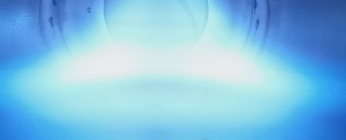


Designed and built by researchers at the Center for Development of Functional Materials, the device is much cheaper than the conventional technology (photo: CDMF)
Published on 09/27/2021
FAPESP Innovative R&D* – Researchers at the Center for Development of Functional Materials (CDMF), one of the Research, Innovation and Dissemination Centers (RIDCs) supported by FAPESP, have designed and built an innovative electron beam irradiation machine that can be used in studies of modifications to semiconductor materials, opening up new lines of research in catalysis, photocatalysis, sensors, anti-microbials, magnetic materials and anti-tumor materials, among others.
The machine costs about USD 80,000, significantly less than machines that use conventional electron beam technology, priced in the range of USD 500,000 to USD 3 million.
“We created a midscale semi-industrial machine by reusing parts from devices in our lab that weren’t working any longer, like a scanning electron microscope. In practice, the low-cost machine changes how novel semiconductors are produced by electron irradiation. We’ve already patented a method of obtaining semiconductors and will now file for an international patent on this innovation,” says Elson Longo, Executive Director of CDMF.
According to Longo, recent years have seen a significant rise in demand for new materials whose properties and functions can be manipulated via novel synthesis routes or modified by physical and/or chemical methods. In particular, modifications to materials using electron irradiation under a scanning and transmission electron microscope have been extensively used not only as morphological characterization platforms but also as a technique for the processing and fabrication of new materials.
The technique achieves very precise modification of materials by controlling energy use, incidence angle and exposure time. Correct use of these parameters leads to structural defects in the material, permitting the enhancement or creation of properties that cannot be obtained by conventional chemical or physical means.
Research on modification of materials by electron beam microscopy has been conducted for years by scientists at CDMF, which is hosted by the Federal University of São Carlos (UFSCar). Through close collaboration with theoretical and simulation groups, they have succeeded in predicting the properties of these materials according to the energy dose applied, shortening the time taken to develop innovative high-tech materials.
A major challenge in materials processing is making production scalable and economically feasible via a satisfactory cost-benefit ratio and an easy fabrication procedure. This necessity led to the design and development of the electron beam irradiation machine so that reactions do not have to be performed only in electron microscopes and can be applied in a range of research fields.
The electron beam irradiation system developed at CDMF was designed to run at a high electron acceleration voltage for rapid modification of materials (in minutes) and has a larger irradiation area for large-scale production.
“The device reduces processing time and uniformly distributes the energy of the electron beam so that the irradiated materials can be reproduced by controlling parameters such as irradiation atmosphere [gas injection and mixture] or acceleration anode voltage, which can’t be controlled with existing methods. In addition, electrical measurements can be taken on the material itself during the irradiation process,” says João Paulo de Campos da Costa, a doctoral researcher at CDMF supervised by Longo and João Paulo Pereira do Carmo, a professor in the Department of Electrical Engineering at the University of São Paulo’s São Carlos School of Engineering (EESC-USP).
Costa is conducting his PhD research in collaboration with Adenilson Chiquito and Leonélio Cichetto Júnior, professors in UFSCar’s Department of Physics, and Juan Andrés, a professor at Spain’s Jaume I University. Like Costa, all three are also affiliated with CDMF.
Different interactions
The machine was meticulously designed for different types of interaction between radiation and material so that it can be used to modify many types of material. Besides performing electron beam irradiation, it can be coupled to an excimer laser (a form of ultraviolet laser) attached to a pulsed laser deposition (PLD) machine belonging to CDMF and used to irradiate and modify samples by means of a technique that combines a nanosecond laser beam with the electron beam.
Several scientific papers published by the CDMF researchers address the topic of modifying the physical and chemical properties of materials by irradiating them with a femtosecond laser that emits ultrashort pulses (a femtosecond is a quadrillionth of a second). To further this research, the device can also be coupled to a femtosecond laser as an external source, enabling materials to be irradiated in an ultrahigh vacuum and controlled atmosphere.
Promising applications involving materials irradiated with the innovation include antiviral surface coating against SARS-CoV-2, among others, biosensors for medical diagnosis with heightened sensitivity, and superefficient materials for dye and pollutant degradation. Novel materials and structures not yet reported in the literature can also be created.
* With information from CDMF’s press office.
Source: https://agencia.fapesp.br/36932