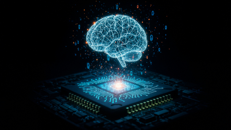
Unlike conventional computers, in which processing and memory are separate, neuromorphic computing seeks to integrate these functions onto a single physical substrate, similar to biological synapses (image: Freepik/Magnific)
Published on 06/30/2026
By José Tadeu Arantes | Agência FAPESP – Neuromorphic computing is a computational paradigm that mimics the way the brain functions in terms of both architecture and dynamics. It creates electronic circuits that store and process information in an integrated manner, similar to networks of neurons and synapses.
With this goal in mind, an international network of researchers developed an electronic device, including Victor López-Richard, a full professor at the Center for Exact Sciences and Technology at the Federal University of São Carlos (CCET-UFSCar) in Brazil. The result, published in Nature Communications, represents an important contribution to the development of neuromorphic computing.
Unlike conventional computers, in which processing and memory are separate, neuromorphic computing seeks to integrate these functions onto a single physical substrate, similar to biological synapses.
“The device is based on the interface between two oxides: LaAlO₃ [lanthanum aluminum oxide] and SrTiO₃ [strontium titanate]. At that interface, a quasi two-dimensional electron gas forms and acts as a conductive channel that can be electrically modulated. The result is essentially a transistor, but one that can also function as a memristor and a memcapacitor,” Lopez-Richard explains.
A transistor controls the flow of electric current in a circuit, functioning as a switch or amplifier. A resistor impedes the flow of current, and a capacitor stores electric charge and releases it later. In the developed device, these functions are combined with an additional element: memory. Thus, in addition to acting as a transistor, the device can function as a memristor, a resistor whose resistance depends on the history of applied signals, and a memcapacitor, a capacitor whose capacitance also depends on the history of the system.
This dependence on the past brings these components closer to the behavior of synapses. Furthermore, the device has an unusual architecture and mode of operation. “In terms of architecture, the unique feature is that it has control gates on the sides instead of the traditional configuration with the gate over the channel found in conventional MOSFETs,” says López-Richard.
A MOSFET (metal-oxide-semiconductor field-effect transistor) is a type of transistor that controls, amplifies, or switches electrical signals. With three main terminals – the gate, which controls the device; the source, through which electrons enter; and the drain, through which electrons exit – it functions as a kind of “electrical faucet.” The voltage applied to the gate determines whether current can flow between the source and drain.
The device in question has a different configuration.
In terms of operation, it is an analog component in a world dominated by digital technology. “Analog operation allows it to function in multiple intermediate states rather than just two – on or off – as in conventional digital transistors,” the researcher explains.
A central focus of the work is to identify the physical mechanism responsible for memory. While the two-dimensional electron gas is crucial for conduction, it is not the main carrier of memory. “This gas influences memory, but the state variable that defines the memory effect is the charges stored in the side gates. They control the conduction channel,” says López-Richard. The accumulation of charges in the side gates occurs gradually and in a controlled manner, modulating the conduction channel through electrostatic effects. This mechanism differs from the one often attributed to memory devices, which is based on the migration of oxygen vacancies.
The main innovation of this work is electronic polymorphism, which is the ability of a single device to perform multiple functions. The function changes based solely on the electrical connection configuration. “Simply connecting or disconnecting a port is enough to change the function,” the researcher summarizes. According to the authors, integrating functions can significantly reduce the number of interconnections and energy consumption, which are the main bottlenecks in current computing.
The study demonstrated the effectiveness of the device in various brain-inspired functionalities, such as reservoir computing and the ability to recognize simple patterns, like digits from 0 to 9 in low-resolution images, by exploiting nonlinearity and short-term memory. The device also exhibits synaptic plasticity, the ability to strengthen a response temporarily or permanently following repeated stimuli, as occurs during learning. Additionally, the device has reconfigurable logic, which involves performing and storing logical operations, such as “and,” “or,” and “not,” directly within the device itself without the need for external memory. Furthermore, analyses indicate energy consumption per operation in the range of a few nanojoules, which is lower than that of equivalent conventional architectures.
Long-standing collaboration
Despite this advance, the authors emphasize that the work is still in its early stages. “What we’re presenting now are proofs of concept, in line with basic research. To develop a commercial product, we must overcome several challenges, such as achieving scalability, integrating with existing technologies, and controlling variability among devices,” Lopez-Richard acknowledges.
The work is the result of an international scientific collaboration that has been developing for over a decade. “Our partnership with the University of Würzburg [Julius-Maximilians-Universität Würzburg, JMU] in Germany began with a project funded by FAPESP between 2013 and 2015. The project has been completed, but the collaboration continues,” says López-Richard.
The present study was supported by FAPESP through the Regular Project “Harnessing the Effects of Memory in Nanostructured and Semiconductor Systems” and a Grant for Scientific Meetings Abroad.
In a complementary study published in Applied Physics Letters and selected as a “featured article” by the editors, the group deepened its understanding of the capacitive memory properties of these systems. “In that work, we combined experimental results and theoretical modeling to demonstrate that analog memcapacitance is governed by charge localization mechanisms in lateral floating gates, enabling precise and reversible control of the capacitive characteristics. Those findings are fundamental to the development of low-power, high-efficiency memory devices,” says López-Richard. This work was also supported by FAPESP.
The article “Oxide interface-based polymorphic electronic devices for neuromorphic computing” can be found at nature.com/articles/s41467-026-71642-2.
Source: https://agencia.fapesp.br/58555
