


Combining materials in a heterostructure is particularly interesting because it can improve electron separation and transport (image: CDMF)
Published on 08/19/2026
Agência FAPESP* – A Brazilian team of scientists has made a significant breakthrough in the synthesis of functional materials by developing, for the first time, a simple and efficient technique for producing metal-semiconductor heterostructures using an ultrashort-pulse laser.
The research, conducted by scientists at the Center for the Development of Functional Materials (CDMF), may lead to new applications in photocatalysis, optoelectronics, and photonics. The CDMF was a FAPESP Research, Innovation, and Dissemination Center (RIDC) active from July 2013 to July 2026, a period during which it was based at the Federal University of São Carlos (UFSCar).
The study was published in the journal Materials Today Chemistry and describes an innovative method that uses femtosecond lasers (each pulse lasting one trillionth of a second) to transform a single precursor material into a complex heterostructure.
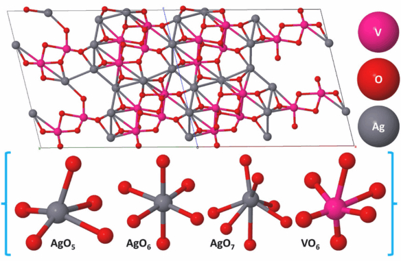
The researchers were able to simultaneously produce three distinct phases of a semiconductor material known as silver orthovanadate (Ag₃VO₄) by irradiating it with femtosecond laser pulses: Ag₃VO₄, a p-type semiconductor; β-AgVO₃, an n-type semiconductor; and metallic silver (Ag₀) with plasmonic properties.
The combination of these materials in a heterostructure is interesting because it can improve electron separation and transport, which is essential for the efficiency of photocatalytic and optoelectronic devices. Furthermore, the presence of metallic particles with a plasmonic effect can broaden the visible light absorption response.
Traditionally, producing metal-semiconductor heterostructures requires complex, multi-step, costly processing methods. The approach reported by the CDMF group uses the ultrafast interaction between light and matter to induce non-thermal transformations in the material and generate hybrid structures directly from a single precursor.
Advantages and scientific impact
The technique offers significant advantages. For example, it is simple and efficient because only one step is required to create multiphase structures. Another advantage is precise structural control because the laser pulses interact with the material in such a short amount of time that they prevent unwanted thermal damage.
Additionally, these materials have potential technological applications in energy conversion systems, advanced sensors, and light-activated catalysts.
The work underscores the importance of collaboration among materials science, physics, and chemistry researchers to address key challenges in modern materials science. As the authors highlight, the methodology opens new avenues for exploring surface and interface engineering with a direct impact on energy and environmental research.
The article “From p-type to n-type semiconductor and metallic material: a one-step route using femtosecond pulsed laser to produce Ag3VO4/Ag3VO3/Ag heterostructure” can be read at sciencedirect.com/science/article/abs/pii/S2468519425002289.
* With information from the CDMF
Source: https://agencia.fapesp.br/59019


